
Subscribe to get the latest news and updates. No span, we promise.

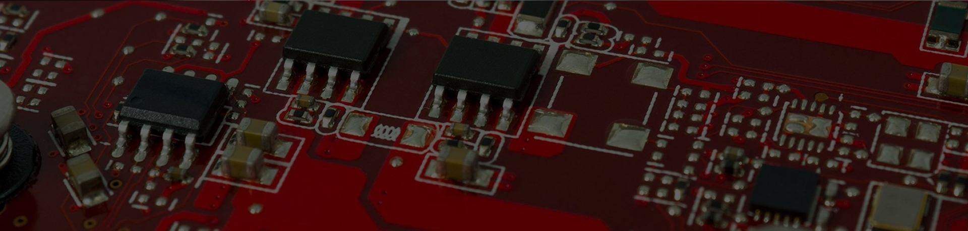
Sierra Assembly manufactures multilayer printed circuit boards for electronic designs that require multiple conductive layers within a compact board structure. Our multilayer PCB fabrication capabilities support prototype development, low-volume requirements, and production programs, with board construction based on your electrical, mechanical, and application requirements.
From initial design review through completed bare-board production, we work with you to evaluate layer count, stack-up, material selection, board thickness, copper requirements, surface finish, and other manufacturing specifications. Our Chino, California facility provides U.S.-based engineering support for projects that require practical guidance throughout the PCB fabrication process.
With 30+ years of industry experience, ISO 9001:2015 and AS9100D certifications, and ITAR registration, we provide multilayer PCB manufacturing support for customers requiring consistent board construction and dependable production.

A multilayer PCB combines several conductive layers with insulating materials to create additional routing space without increasing the overall board footprint. This construction is useful when a design requires more circuitry, dedicated power and ground layers, or complex interconnections within a limited area.
We fabricate multi-layer circuit boards according to your design files and specified construction requirements. Depending on the project, fabrication considerations can include:
Our engineering team reviews these details before production to help identify potential fabrication concerns.
We provide fabrication support for different multilayer board constructions and production requirements.
|
Capability |
Our Support |
|---|---|
|
Multilayer PCB Fabrication |
Bare-board production based on your design and construction specifications |
|
Prototype Fabrication |
Initial boards for design verification and product development |
|
Low-Volume Manufacturing |
Small quantities and repeat fabrication requirements |
|
Production Manufacturing |
Larger production runs based on your required quantities |
|
Layer Stack-Up |
Construction based on your specified layer arrangement |
|
Material Selection |
FR-4, High-Tg, and applicable specialty materials |
|
Copper Construction |
Inner and outer layer copper requirements based on the design |
|
Board Thickness |
Finished thickness based on your mechanical requirements |
|
Surface Finish |
Finish options selected according to board requirements |
|
DFM Review |
Manufacturing review before fabrication begins |
|
Electrical Testing |
Testing based on your project and quality requirement |
The stack-up determines how the conductive and dielectric layers are arranged within a multilayer board. A suitable construction can help accommodate routing, power distribution, signal requirements, and mechanical constraints.
Your multilayer stack-up may include:
We review the proposed construction against your board specifications and manufacturing requirements. Where applicable, our engineering team can identify areas that may require attention before the design moves into production.
Material selection plays an important role in the electrical, thermal, mechanical, and manufacturing characteristics of a multilayer circuit board.
|
FR-4 |
General-purpose multilayer PCB applications |
|
High-Tg Materials |
Designs requiring increased thermal performance |
|
Specialty Materials |
Applications with specific electrical or environmental requirements |
|
Core Materials |
Determined by the required multilayer construction |
|
Prepreg |
Used to build the required dielectric structure |
|
Copper Foil |
Selected according to layer and electrical requirements |
Every multilayer board has construction requirements that influence its fabrication. We work from your specified parameters to produce boards suited to the intended application.
Common specifications include:
Providing complete specifications at the quotation stage helps our team evaluate the manufacturing requirements accurately.
Multi-layer circuit boards are used across applications where a single- or double-sided construction cannot provide the required routing capacity or board density.
A properly designed multilayer board can provide several advantages for complex electronic products:
To evaluate your project, our team typically needs the following information:
|
Required Information |
Details |
|---|---|
|
PCB Design Files |
Gerber or ODB++ files |
|
Layer Count |
Number of conductive layers |
|
Board Dimensions |
Required finished board size |
|
Material |
FR-4, High-Tg, or specified specialty material |
|
Board Thickness |
Required finished thickness |
|
Copper Weight |
Inner and outer layer copper requirements |
|
Stack-Up |
Layer arrangement and dielectric construction when available |
|
Surface Finish |
Required surface finish |
|
Quantity |
Prototype, low-volume, or production quantity |
|
Testing |
Required electrical testing and inspection |
|
Delivery Requirements |
Target production and delivery timeline |
Have your design files ready? Send your multilayer PCB specifications to Sierra Assembly for a manufacturing review and quote.
When you need a multilayer PCB manufacturer, you need a partner that can understand both your design requirements and the realities of production.
Sierra Assembly provides:
1. What is multilayer PCB fabrication?
Ans: Multilayer PCB fabrication is the process of manufacturing a circuit board that contains multiple conductive layers separated by dielectric materials. The layers are combined into a single board structure to provide additional routing and circuit capacity.
2. What materials are available for multilayer PCB manufacturing?
Ans: We support FR-4, High-Tg, and applicable specialty materials based on your design, thermal requirements, electrical performance, operating environment, and application.
3. How many layers can you fabricate?
Ans: Layer requirements depend on the specific board design and manufacturing capabilities applicable to your project. Our engineering team can review your design files and required stack-up to determine an appropriate fabrication approach.
4. Can you fabricate prototype multilayer PCBs?
Ans: Yes. We support prototype fabrication so you can evaluate your board design and construction before moving into low-volume or production quantities.
5. Do you support low-volume multilayer PCB manufacturing?
Ans: Yes. We support prototype, low-volume, repeat, and production manufacturing requirements based on your project specifications.
6. What files are required to manufacture a multilayer PCB?
Ans: We typically need Gerber or ODB++ files along with layer count, board dimensions, material, thickness, copper weight, stack-up information, surface finish, quantity, testing requirements, and delivery requirements.
7. Can Sierra Assembly also provide PCB assembly?
Ans: Yes. PCB assembly can be provided when your project requires components to be placed and soldered onto the fabricated board. Assembly requirements can be evaluated separately based on your BOM and assembly documentation.
8. How long does multilayer PCB fabrication take?
Ans: Turnaround depends on layer count, board construction, materials, quantity, testing requirements, and other project specifications. A 24-hour turnaround may be available for qualifying projects following project review.
Use our onlinePCB assembly cost calculator and quote PCB assembly online as per your specifications. Save your time with our PCB Assembly instant Online Quote.
Download our brochure to know more about capabilities.
If you find that your project doesn’t fit within our online configurator, fill out the form with your specific needs , upload files and we will create a customized quote for you.
Custom Quote