High Frequency PCB Manufacturer for Reliable RF & High-Speed Applications in Chino, California
Modern electronic systems require stable signal transmission, low signal loss, and reliable electrical performance at elevated frequencies. Sierra Assembly Technology is a trusted high frequency PCB manufacturer providing advanced fabrication and assembly solutions for RF, microwave, and high-speed electronic applications.
Our high frequency PCB services support advanced materials including Rogers and PTFE-based laminates, controlled impedance designs, multilayer PCB configurations, and precision manufacturing processes designed for demanding electronic systems.
With responsive engineering support, fast-turn manufacturing capabilities, and quality-focused production processes, we help simplify the transition from prototype development to scalable production manufacturing.
Why Manufacturers Choose Sierra Assembly Technology
-
30+ Years of Electronics Manufacturing Experience
-
AS9100 Rev-D & ISO 9001:2015 Certified Processes
-
RoHS-Compliant Manufacturing Support
-
Fast-Turn Manufacturing Available
-
Prototype to Production Support
-
U.S.-Based Engineering & Manufacturing Team
-
Responsive Customer & Engineering Communication
-
Quality-Focused Manufacturing Processes
Whether you require a high frequency printed circuit board for telecommunications, aerospace, automotive electronics, industrial automation, or medical devices, our experienced team delivers reliable manufacturing solutions tailored to your project requirements.
Common Materials for High Frequency PCB
Material selection plays an important role in high frequency PCB performance, signal stability, and electrical reliability. Unlike standard FR4 boards, high frequency PCBs use low-loss materials designed to reduce signal attenuation and improve high-speed performance.
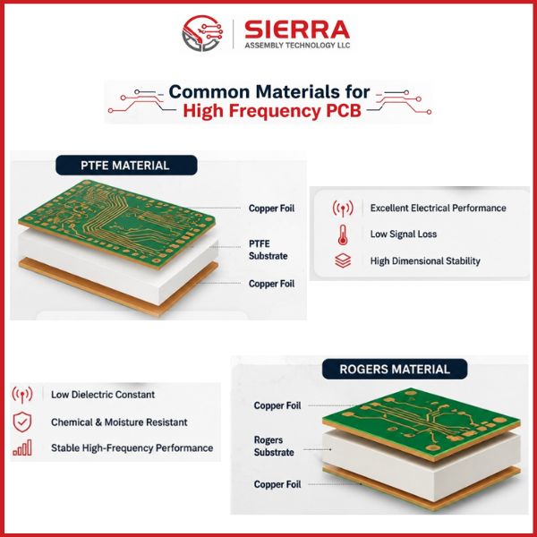
Rogers PCB Materials
Rogers materials are widely used in high frequency PCB design for RF and microwave applications requiring stable electrical performance and reliable signal integrity. These materials support controlled impedance, thermal stability, and multilayer PCB integration for high-speed electronic systems.
PTFE (Teflon-Based Materials)
PTFE-based PCB materials are commonly used in high frequency circuit boards requiring low dielectric loss, strong thermal performance, and stable signal transmission. These materials help improve RF performance while supporting reliable operation in demanding electronic applications.
Types of High Frequency PCBs
Sierra Assembly Technology supports multiple types of high frequency PCBs designed for RF, microwave, and high-speed electronic applications requiring reliable signal performance and advanced PCB integration.
-
Rigid High Frequency PCBs: Rigid high frequency PCBs are commonly used in communication systems, industrial electronics, automotive technologies, and RF applications requiring stable mechanical support and reliable electrical performance.
-
Flexible & Rigid-Flex High Frequency PCBs: Flexible and rigid-flex PCB solutions support compact electronic devices requiring bending capability, space optimization, and advanced circuit integration.
-
RF & Microwave PCBs: RF and microwave PCBs are designed for high-speed signal transmission in wireless communication systems, radar technologies, satellite communication, and 5G infrastructure.
-
Multilayer High Frequency PCBs: Multilayer high frequency circuit boards support high-density routing, controlled impedance, and complex electronic systems requiring improved signal integrity and compact PCB layouts.
Benefits of High Frequency PCBs
Low Signal Loss: Advanced PCB materials help reduce signal attenuation and improve electrical performance in high-speed applications.
Stable High-Speed Performance: High frequency PCBs support reliable signal transmission and consistent performance in RF and high-speed electronic systems.
Improved Signal Integrity: Controlled impedance and low-loss materials help minimize interference, signal reflection, and transmission delays.
High Frequency PCB Manufacturing Capabilities
|
Capability
|
Details
|
|
PCB Stack-Up Support
|
Custom multilayer PCB stack-up configurations
|
|
High-Speed PCB Materials
|
Support for advanced high-speed PCB materials
|
|
High Frequency PCB Materials
|
Rogers & PTFE-based material support
|
|
Controlled Impedance Support
|
Controlled impedance PCB design and manufacturing support
|
|
Multilayer PCB Capabilities
|
Multilayer high frequency PCB manufacturing
|
|
PCB Fabrication Support
|
Precision PCB fabrication for RF & high-speed applications
|
|
PCB Assembly Services
|
SMT, Through-Hole & Mixed Technology Assembly
|
|
Signal Integrity Support
|
Manufacturing support for reliable signal transmission
|
|
Prototype to Production
|
Engineering prototypes to scalable production manufacturing
|
|
Testing Capabilities
|
X-Ray Inspection & Functional Testing
|
|
Industry Applications
|
Telecommunications, Aerospace, Medical, Automotive & Industrial Electronics
|
High Frequency PCB Design Considerations
-
Controlled Impedance: Controlled impedance helps maintain signal integrity and reliable signal transmission in RF and high-speed electronic applications.
-
Material Stability: Selecting the right high frequency PCB materials helps improve thermal stability, electrical performance, and long-term reliability.
-
Copper Foil & Surface Finish: Proper copper foil selection and surface finishes help improve signal stability, conductivity, and overall PCB reliability.
Common Applications of High Frequency PCBs
-
RF & Microwave Systems: High frequency PCBs are widely used in RF and microwave applications requiring stable signal transmission and minimal signal distortion.
-
5G Infrastructure: High frequency circuit boards support high-speed communication systems, wireless networking equipment, and advanced 5G technologies.
-
Satellite Communication: Advanced high frequency PCB materials help support reliable signal performance in satellite and aerospace communication systems.
-
Aerospace & Defense: Used in radar systems, military communication equipment, avionics, and mission-critical electronic applications.
-
Medical Electronics: Supports imaging systems, diagnostic devices, monitoring equipment, and advanced medical technologies.
Prototype to Production Support
Sierra Assembly Technology supports the complete product development lifecycle from prototype fabrication to scalable production manufacturing. Whether you are launching a new RF product or refining an existing design, our flexible manufacturing approach helps simplify the transition from engineering development to full production.
Our manufacturing capabilities support engineering prototypes, pilot production, low-volume builds, high-mix manufacturing, and scalable production requirements while maintaining consistent quality and responsive production support.
Our Prototype to Production Support Includes:
-
New Product Introduction (NPI) Support
-
Engineering Prototype Manufacturing
-
Design Validation Support
-
Low-Volume & High-Mix Production
-
Production Scaling Support
-
Faster Time-to-Market
-
Manufacturing & Assembly Coordination
-
Ongoing Production Support
Why Choose Sierra Assembly Technology?
Choosing the right high frequency PCB supplier directly impacts signal performance, manufacturing reliability, and overall product success.
At Sierra Assembly Technology, we combine advanced PCB manufacturing capabilities, responsive engineering communication, and quality-focused production processes to support complex high frequency PCB projects for demanding industries.
Our experienced team works closely with engineering and product development teams to help improve manufacturing efficiency, reduce delays, and accelerate product launches.
Frequently Asked Questions
1. What is a high frequency PCB?
Ans: A high frequency PCB is a specialized circuit board designed for RF and high-speed electronic applications requiring controlled impedance and reliable signal transmission.
2. What materials are commonly used in high frequency PCBs?
Ans: Common high frequency PCB materials include Rogers PCB materials and PTFE (Teflon-based) materials designed for stable RF performance and low signal loss.
3. Do you provide high frequency PCB assembly services?
Ans: Yes. Sierra Assembly Technology provides complete high frequency PCB assembly support including SMT assembly, multilayer PCB integration, and RF PCB manufacturing services.
4. Can you support prototype and low-volume projects?
Ans: Yes. We support engineering prototypes, low-volume builds, high-mix production, and scalable manufacturing requirements.
5. Do you support controlled impedance PCB manufacturing?
Ans: Yes. Our controlled impedance PCB support helps improve signal integrity and electrical stability for high-speed and RF applications.
Start Your High Frequency PCB Project Today
If you are looking for a reliable high frequency PCB supplier and manufacturer for RF, microwave, and high-speed electronic applications, Sierra Assembly Technology is ready to support your project with advanced manufacturing expertise, responsive engineering support, and dependable production capabilities.
Request a Quote Today | Upload Your Files | Speak with Our Engineers