
Subscribe to get the latest news and updates. No span, we promise.

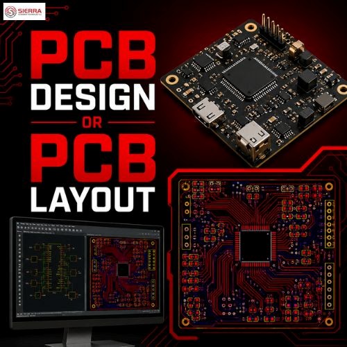
With the evolution of new technologies and miniaturization of electronics, PCBs used in them have become compact and demands sophistication.
Use our onlinePCB assembly cost calculator and quote PCB assembly online as per your specifications. Save your time with our PCB Assembly instant Online Quote.
Download our brochure to know more about capabilities.
If you find that your project doesn’t fit within our online configurator, fill out the form with your specific needs , upload files and we will create a customized quote for you.
Custom Quote