Multilayer PCB Assembly Services
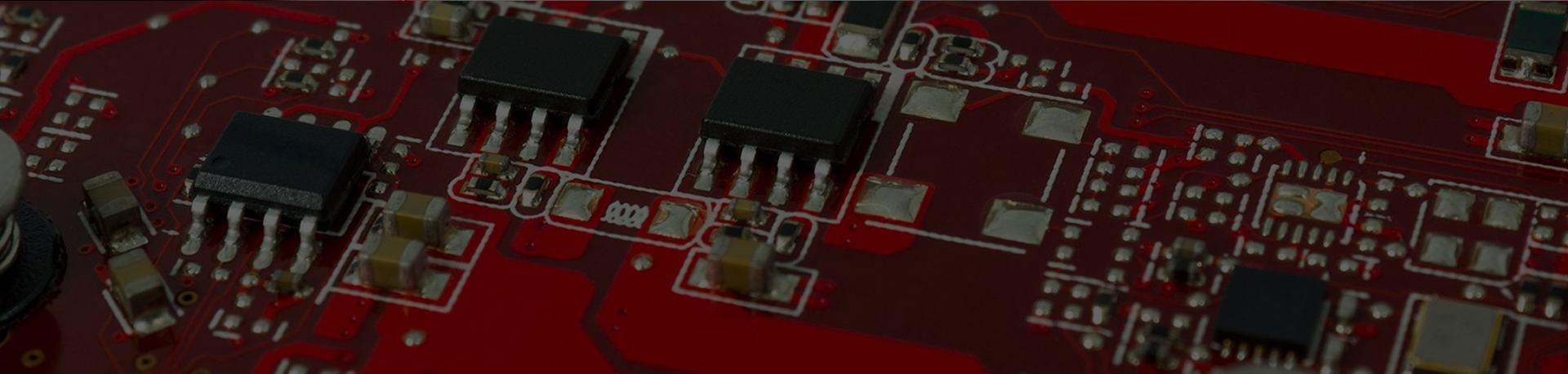
At Sierra Assembly Technology, we specialize in Multilayer PCB Assembly, providing precision, reliability, and high-performance solutions for complex electronic designs. As devices become smaller and more sophisticated, multilayer PCBs have become essential for industries requiring high-density circuits, signal integrity, and robust mechanical strength.
With decades of experience and U.S.-based manufacturing, we help customers transform complex PCB designs into production-ready, dependable solutions.
What Are PCB Assembly Services?
PCB Assembly Services involve mounting and soldering electronic components onto printed circuit boards to create fully functional circuits. For
multilayer PCBs, which contain three or more layers of copper and insulating materials, assembly is critical to ensure signal performance, thermal management, and long-term reliability.
At Sierra, our
custom multilayer PCB assembly services ensure each project meets quality, compliance, and performance standards while supporting both prototypes and full-scale production.
Why Multilayer PCB Assembly Matters
The quality of
Multilayer PCB Assembly directly affects your product’s performance. Poor assembly can cause signal loss, thermal stress, or premature failure, especially in high-reliability industries such as aerospace, medical, or industrial electronics.
By choosing a trusted
multilayer pcb assembly Manufacturer like Sierra, customers benefit from:
-
Reduced failure rates
-
Improved signal integrity
-
Faster time-to-market
-
Compliance with industry standards
Types of Multilayer PCB Assembly Services We Offer
Sierra provides a range of
multilayer PCB assembly services tailored to your design and production needs:
|
Type
|
Description
|
Best For
|
|
SMT Assembly
|
High-speed placement of surface-mount components
|
Compact, high-density boards
|
|
Through-Hole Assembly
|
Soldering pin-in-hole components
|
Mechanical stability & connectors
|
|
HDI PCB Assembly
|
Microvias, fine-pitch components
|
Advanced electronics & wearables
|
|
Mixed Technology Assembly
|
Combination of SMT and through-hole
|
Complex multilayer designs
|
Why choose Sierra? We combine
advanced equipment, quality controls, and U.S.-based engineering support to deliver unmatched precision and reliability.
Our Multilayer PCB Assembly Process
At Sierra Assembly Technology, our multilayer PCB assembly process is designed to deliver precision, reliability, and long-term performance. Each step in our workflow is optimized for high-density, complex multilayer PCBs, ensuring that your boards perform flawlessly in demanding applications like aerospace, medical, and industrial electronics.
1. Material & Component Preparation
The foundation of a successful
multilayer PCB assembly begins with proper material handling.
-
BOM Validation: Our engineers carefully review the Bill of Materials (BOM) to ensure accuracy and compatibility of components. This step prevents assembly errors and ensures smooth production.
-
Component Inspection: All components are visually and electronically inspected for defects, orientation, and functionality.
-
Moisture-Sensitive Component Handling: Certain components, such as BGAs and ICs, are moisture-sensitive. We follow strict handling and baking procedures to prevent soldering defects.
-
Inventory & Traceability: Each component is tracked using U.S.-based inventory systems for traceability, ensuring quality and compliance throughout the assembly.
2. Solder Paste Printing
Accurate solder paste application is critical for reliable SMT
multilayer PCB assembly.
-
Precision Stencil Printing: Using laser-cut stencils, solder paste is applied uniformly on all pads. This ensures strong electrical and mechanical connections for surface-mount components.
-
Print Inspection: Our automated solder paste inspection (SPI) system checks the paste volume, alignment, and placement, minimizing defects before components are placed.
3. Automated Component Placement
High-speed, precise placement of surface-mount devices (SMDs) is crucial for
multilayer PCB assembly.
-
Pick-and-Place Machines: Our advanced machines place components with micron-level accuracy.
-
Handling Fine-Pitch & HDI Components: Our process supports high-density boards, micro-BGA, and fine-pitch components.
-
Optimized Placement: Components are placed according to design files and verified for correct orientation.
4. Reflow Soldering
Once components are in place,
reflow soldering permanently bonds them to the PCB.
-
Controlled Thermal Profiles: Each multilayer PCB is carefully heated through preheat, soak, and reflow zones to prevent warping or thermal damage.
-
High-Quality Solder Joints: Our process ensures consistent solder joints across all layers, critical for high-speed signals and reliability.
-
Support for Lead-Free Soldering: We comply with RoHS standards, using lead-free solder to meet environmental regulations.
5. Through-Hole & Selective Soldering
For mechanical stability or larger components,
through-hole assembly is performed:
-
Wave Soldering / Selective Soldering: Components like connectors, transformers, or pins are soldered using wave or selective methods.
-
Enhanced Board Strength: This step reinforces multilayer structures and ensures reliable electrical connections through the layers.
-
Critical Applications: Especially important in aerospace, industrial, or medical electronics where durability is paramount.
6. Inspection & Testing
Quality control is integrated into every stage of our
multilayer PCB assembly process.
-
Automated Optical Inspection (AOI): Identifies missing, misaligned, or defective components.
-
X-Ray Inspection: Critical for hidden joints, such as BGAs or buried vias, ensuring interlayer connectivity.
-
In-Circuit Testing (ICT): Verifies electrical functionality, detecting shorts, opens, and resistance issues.
-
Functional Testing: Simulates real-world operating conditions to confirm board performance before delivery.
7. Final QA & Packaging
The last step ensures that every board meets the highest standards before shipment:
-
Visual & Dimensional Checks: Ensures boards match specifications exactly.
-
Cleanliness & Protective Coating: Boards are cleaned to remove flux residue and packaged with protective anti-static materials.
-
Traceable Documentation: All test and inspection reports are included for customer records.
-
On-Time Delivery: Boards are carefully packaged to prevent damage during transit.
How to Make a Multilayer PCB
While assembly is critical, the
fabrication of the multilayer PCB is equally important. At Sierra, we fabricate boards using advanced techniques:
-
Etching inner layers to form precise copper circuits
-
Stacking layers with prepreg and outer copper foils
-
Drilling vias and plating for interlayer connectivity
-
Applying solder mask, silkscreen, and surface finish
-
Testing the bare board for electrical integrity
This ensures a
strong foundation for our
multilayer PCB assembly services.
Sierra offers advanced Advanced Capabilities for Multilayer PCB Assembly
|
Capability
|
Description
|
|
High-density SMT
|
Placement of fine-pitch components and BGA/µBGA
|
|
Lead-free & RoHS
|
Compliant assembly for environmental safety
|
|
HDI Support
|
Microvias and high-speed signal integrity
|
|
Flexible Volume
|
Prototypes to full-scale production runs
|
We are a full-service
multilayer PCB manufacturer, providing everything from fabrication to assembly under one roof.
Specifications & Materials
Our multilayer PCB assembly services support a wide range of specifications and materials, ensuring each board meets the unique requirements of your application.
|
Parameter
|
Range / Options
|
|
Layer Count
|
4 to 12+ layers
|
|
Materials
|
FR-4, High-TG laminates, specialty materials
|
|
Board Thickness
|
Custom per application
|
|
Copper Weight
|
Standard & heavy copper
|
|
Compliance
|
RoHS, Lead-free manufacturing
|
Difference Between Single-Layer & Multilayer PCB
Multilayer PCBs allow higher component density, better signal integrity, and smaller form factors.
|
Feature
|
Single-Layer PCB
|
Multilayer PCB
|
|
Layers
|
1
|
3+
|
|
Complexity
|
Simple
|
High
|
|
Signal Integrity
|
Limited
|
Excellent
|
|
EMI Control
|
Minimal
|
Advanced
|
|
Board Size
|
Larger for complex circuits
|
Compact
|
|
Applications
|
Simple electronics
|
Advanced devices
|
Applications of Multilayer PCB Assembly
-
Aerospace & defense (avionics, control systems)
-
Medical & healthcare (diagnostics, monitors)
-
Telecommunications & wireless systems
-
Industrial automation & controls
-
Consumer electronics & wearables
Benefits of Multilayer PCB Assembly
-
High-performance designs for advanced electronics
-
Compact & space-saving boards for wearables and smart devices
-
Durable & reliable for harsh environments
-
Advanced technology support including HDI and fine-pitch assembly
-
Custom & scalable solutions from prototypes to production
-
Quality assured with strict inspection and testing
Industries That Benefit
|
Industry
|
Applications
|
|
Aerospace & Defense
|
Satellite and avionics boards
|
|
Medical
|
Monitoring and imaging devices
|
|
Telecommunications
|
RF and high-speed systems
|
|
Industrial
|
Robotics, sensors, automation
|
|
Consumer Electronics
|
Smartphones, wearables, LED devices
|
Features of Multilayer PCB Assembly Services
-
U.S.-based manufacturing & support
-
Experienced engineering team
-
Advanced equipment and process control
-
Compliance with RoHS and industry standards
-
Flexible volumes and quick turnaround
Why We Are Different
Sierra Assembly Technology stands out as a
multilayer pcb assembly Manufacturer because:
-
30+ years of PCB manufacturing experience
-
In-house fabrication + assembly capabilities
-
Certified quality systems for aerospace, medical, and industrial sectors
-
U.S.-based customer support for seamless communication
-
Expertise in HDI, fine-pitch, and high-density boards
Our customers trust us as a
multilayer PCB assembly Supplier for precision, reliability, and full-service support.
Partner with Sierra for reliable, high-performance
Multilayer PCB Assembly. From complex prototypes to production-scale runs, we deliver boards built to exacting standards with U.S.-based quality and support.