Subscribe to get the latest news and updates. No span, we promise.

Designing a Printed Circuit Board (PCB) requires both technical expertise and precision. Even small errors can lead to PCB manufacturing problems caused by design, increased costs, delays, or poor product performance. Based on our experience, the top 5 common mistakes are often the source of the majority of errors, while the remaining mistakes are more advanced but critical for high-performance or high-speed designs.
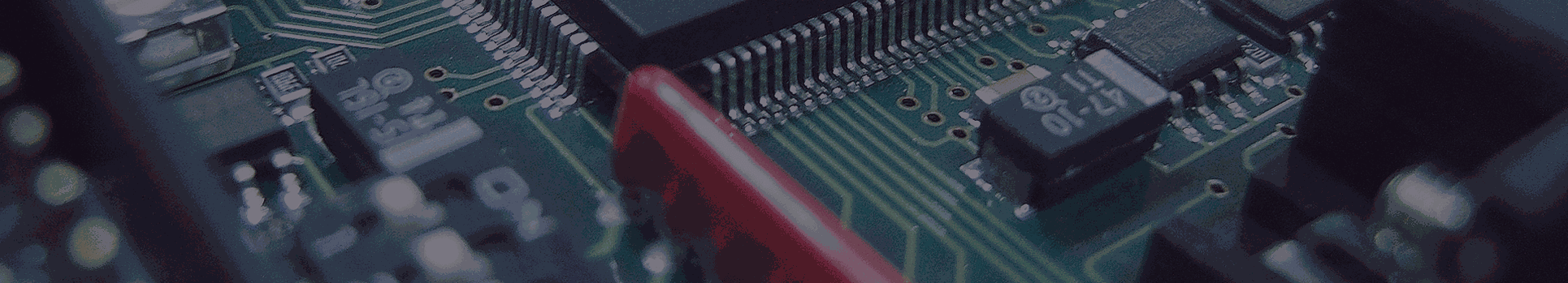
1. Over-Complicated PCB Designs
Complex designs increase the risk of PCB layout errors, signal integrity issues, and higher production costs. Overusing layers or convoluted routing can introduce PCB design violations.
Best Practices:
Impact of Over-Complicated PCB Designs
|
Issue |
Consequence |
Solution |
|
Too many layers |
Higher cost, increased errors |
Limit layers, optimize routing |
|
Complex routing |
Crosstalk, signal delays |
Simplify paths, short direct traces |
|
Poor component grouping |
Difficult debugging |
Group functional blocks |
2. Incorrect Component Placement
Placement mistakes can cause PCB grounding and noise issues, EMI, or signal integrity problems.
Key Tips:
3. Trace Width and Spacing Errors
Incorrect trace width or spacing causes PCB fabrication errors due to poor design, overheating, voltage drops, and PCB layout mistakes.
Considerations:
Trace Width & Spacing Guidelines
|
Trace Type |
Recommended Width |
Notes |
|
Signal |
6–10 mils |
Standard low-power |
|
Power (>0.5A) |
20–40 mils |
Depends on copper thickness |
|
High-speed |
Controlled impedance |
Use simulation tools |
4. Ignoring Design Rule Checks (DRC)
Skipping error checking in PCB design is a major source of PCB layout errors.
Tips:
5. Landing Pattern and Footprint Mistakes
Landing Pattern Errors
|
Error |
Consequence |
Prevention |
|
Wrong pad size |
Poor solder joints |
Follow IPC-7351 |
|
Pin spacing errors |
Component misalignment |
Verify datasheets |
|
Missing footprint |
Assembly failure |
Use verified libraries |
1. Decoupling Capacitor Errors
Improper placement or missing capacitors can lead to PCB power integrity design errors.
2. Via Misuse
Blind, buried, or through-hole vias, if misused, increase PCB fabrication errors due to poor design.
3. High-Speed PCB Design Mistakes
High-speed PCB design mistakes often cause impedance mismatches and signal integrity issues.
4. EMI and Noise Issues
PCB grounding and noise issues arise from poor separation of functional blocks.
5. Antenna and RF Layout Mistakes
Improper layout leads to PCB antenna design mistakes in wireless circuits.
6. Ignoring DFM and Manufacturing Guidelines
Skipping DFM issues in PCB design increases costs and PCB manufacturing problems caused by design.
7. Skipping Design Review
Design reviews catch overlooked errors. Skipping them leads to PCB design violations.
Case Study: Real-World PCB Design Challenges & Sierra Assembly Solutions
|
Difficulty / PCB Issue |
Impact / Consequences |
Sierra Assembly Solution |
|
Signal integrity problems (High-speed trace errors) |
Data loss, reflections, EMI issues |
Recalculated trace width using IPC-2221 standards, optimized spacing, and minimized crosstalk |
|
Power distribution & decoupling capacitor errors |
Voltage fluctuations, unstable IC performance |
Strategically placed decoupling capacitors close to IC pins; optimized power trace routing |
|
Antenna mismatch (Wireless PCB) |
Weak signal, poor communication range |
Corrected antenna placement and orientation; matched impedance to 50Ω for maximum power transfer |
|
Manufacturing delays due to DFM issues |
Misaligned components, soldering failures, higher costs |
Ensured compliance with DFM guidelines for trace widths, pad sizes, and vias |
|
Excessive blind/buried vias |
Increased production cost, potential failure points |
Optimized via selection, minimized blind/buried vias, matched sizes to manufacturer standards |
|
Overall design review skipped |
Undetected design errors reaching production |
Conducted full design review, error checking in PCB design, and simulation tests before fabrication |
Outcome:
Key Takeaway:
Even experienced designers encounter common PCB design errors. Early intervention with professional expertise from Sierra Assembly Technology ensures manufacturable, reliable, and high-performance PCBs.
1. What are the most common PCB design mistakes causing delays?
Ans: Incorrect trace width/spacing, poor component placement, missing decoupling capacitors, landing pattern errors, and ignoring DFM rules.
2. How to avoid high-speed PCB design mistakes?
Ans: Match impedance, minimize trace length, maintain continuous reference planes, and use simulation tools.
3. Why is decoupling capacitor placement important?
Ans: Wrong placement causes voltage fluctuations and unstable ICs; place capacitors close to IC power pins.
4. Consequences of ignoring DFM guidelines?
Ans: Leads to fabrication errors, misaligned components, higher costs, and increased rework.
5. How does Sierra Assembly prevent PCB layout mistakes?
Ans: Through design reviews, DFM checks, simulation, and optimized placement, traces, vias, and decoupling.