Subscribe to get the latest news and updates. No span, we promise.

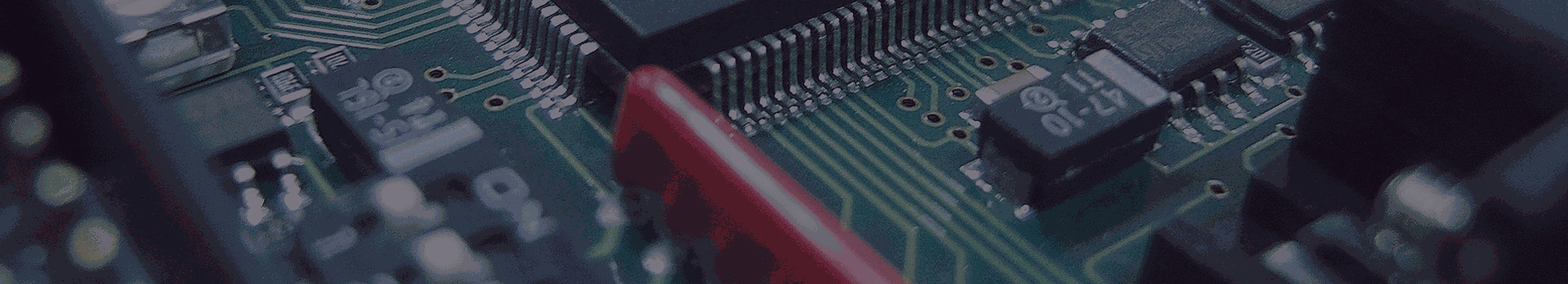
Digitization has become part of everyday life. From smart wearables and medical devices to networking equipment and industrial automation, modern electronics depend heavily on digital systems. Behind every reliable digital product is a well-engineered digital PCB assembly that supports speed, accuracy, and consistent performance.
As demand for connected devices continues to rise, manufacturers are seeing a growing need for PCB assembly for digital electronics that can handle high-speed data, dense layouts, and strict reliability requirements. Over the years, we’ve worked closely with customers designing everything from IoT controllers to high-speed computing systems, and one thing is clear digital PCB assembly requires a very different approach compared to traditional analog boards.
In this article, we break down what digital PCB assembly really means, how it differs from analog assembly, and which design and manufacturing practices help ensure performance, manufacturability, and long-term reliability.
A pcb digital design is built to process discrete signals typically logic “1s” and “0s” at high speed. A digital circuit board assembly consists of integrated circuits, processors, memory devices, connectors, and passive components mounted on a printed circuit board using automated assembly processes.
Unlike basic electronic circuit board assembly, digital PCB manufacturing must account for timing accuracy, signal integrity, and noise control. These assemblies are widely used in:
Because digital systems switch states rapidly, even small layout errors can cause digital PCB signal integrity issues, intermittent failures, or EMI problems that are difficult to debug later.
While both digital and analog boards follow similar fabrication steps, the engineering priorities differ significantly.
Key Differences at a Glance
|
Aspect |
Digital PCB Assembly |
Analog PCB Assembly |
|
Signal Type |
Discrete, high-speed signals |
Continuous signals |
|
Noise Sensitivity |
Lower tolerance for timing errors |
Highly sensitive to noise |
|
Design Focus |
Speed, timing, integrity |
Accuracy and signal purity |
|
Cost Impact |
Optimized via automation |
Often higher due to tuning |
|
Tool Usage |
Heavily software-driven |
More manual validation |
Decoupling capacitors play a critical role in digital PCB design and assembly. In high-speed digital PCB assembly, switching events inside ICs draw sudden bursts of current. Without nearby charge storage, this can cause voltage dips that lead to logic errors. Best practices we follow include:
This approach directly improves power integrity in digital PCB assembly, especially in dense designs.
Routing in digital PCB layout best practices focuses on timing, impedance, and signal isolation. Poor routing is a common source of crosstalk in digital PCB assembly and EMI failures. Routing Guidelines That Matter
|
Design Element |
Common Issue |
Recommended Practice |
|
Clock lines |
Skew, reflection |
Short, direct routing |
|
Data buses |
Timing mismatch |
Length matching |
|
Power traces |
Voltage drop |
Wide, low-impedance paths |
|
Ground plane |
EMI |
Solid, uninterrupted plane |
Effective clock and data signal routing PCB techniques ensure predictable behavior even at higher frequencies.
Smart component placement is one of the most effective digital PCB routing techniques to reduce noise and assembly errors. In digital boards, noisy components such as processors and switching regulators are less sensitive themselves but they can easily interfere with nearby circuits.Placement best practices include:
A clean return path is essential for minimizing EMI and timing errors. Poor grounding is one of the leading causes of EMI issues in digital PCB design. Digital PCB Grounding Essentials
|
Area |
Risk |
Solution |
|
Split ground planes |
EMI, reflections |
Use continuous ground |
|
Via transitions |
Return path disruption |
Add stitching vias |
|
High-speed traces |
Noise coupling |
Route over solid planes |
As data rates increase, digital signal integrity PCB concerns become unavoidable. Issues such as reflections, impedance mismatch, and timing skew directly affect performance.
To avoid digital PCB signal integrity issues, we recommend:
Modern electronic circuit board assembly relies heavily on automation. In digital PCB assembly, software-driven inspection, placement, and testing play a major role in maintaining consistency.
Automation benefits include:
|
Challenge |
Impact |
Mitigation |
|
Crosstalk |
Data corruption |
Proper spacing and routing |
|
EMI |
Compliance failure |
Grounding and shielding |
|
Power noise |
Logic errors |
Robust decoupling |
|
Timing skew |
System instability |
Length matching |
Digital PCB assembly is not just about placing components it’s about understanding how layout, routing, grounding, and manufacturing interact. Over the years, we’ve seen projects fail simply because early design decisions didn’t account for real-world assembly constraints.
Partnering with an experienced provider for digital PCB design and assembly helps avoid costly revisions and ensures a smoother path from prototype to production.
Problem
A U.S.-based IoT startup approached Sierra with a compact digital PCB assembly used in a smart industrial monitoring device. The board included a high-speed microcontroller, clock lines above 500 MHz, multiple sensors, and wireless connectivity.
During early production runs, the customer faced:
These problems directly impacted time-to-market and increased manufacturing costs.
Technical Challenges Identified
|
Area |
Issue Observed |
Impact |
|
PCB Layout |
Long clock traces and poor return paths |
Signal reflection and timing errors |
|
Component Placement |
Congested routing near MCU |
Assembly errors and rework |
|
Power Integrity |
Inadequate decoupling strategy |
Voltage dips during switching |
|
Assembly Readiness |
No panelization optimization |
Slower pick-and-place cycles |
Sierra’s Engineering Solution
Sierra’s design and assembly teams worked collaboratively with the customer to address both design and manufacturing constraints.
Key technical improvements included:
Results Achieved
|
Metric |
Before |
After |
|
PCB Assembly Throughput |
Baseline |
30% faster |
|
Signal Integrity |
Unstable |
Stable across all high-speed lines |
|
EMI Test Results |
Failed |
Passed FCC compliance |
|
Assembly Rework |
High |
Minimal rework required |
1. What makes digital PCB assembly different from analog PCB assembly?
Ans: Digital PCB assembly focuses on high-speed switching signals, clock routing, and noise control, while analog PCB assembly prioritizes signal accuracy, low noise, and stable grounding.
2. Why is signal integrity critical in high-speed digital PCB assembly?
Ans: Poor signal integrity can cause timing errors, data corruption, EMI issues, and unpredictable system behavior, especially at higher clock frequencies.
3. How does PCB design for manufacturability improve assembly speed?
Ans: DFM-optimized designs reduce soldering defects, rework, and component placement issues, resulting in faster, more reliable PCB assembly.
4. What role does component placement play in PCB assembly performance?
Ans: Proper component placement shortens signal paths, improves thermal management, and allows smoother automated assembly with fewer errors.
5. Why should designers involve the PCB assembly team early in the design stage?
Ans: Early collaboration helps identify layout, panelization, and assembly constraints upfront, preventing costly redesigns and production delays.
Digital PCB assembly continues to evolve alongside faster processors, tighter layouts, and smarter devices. By following proven digital PCB layout best practices, addressing power integrity in digital PCB assembly, and controlling EMI and signal integrity from the start, manufacturers can deliver reliable, scalable products. A well-designed digital PCB doesn’t just function it performs consistently, assembles efficiently, and stands up to real-world operating conditions. Looking for reliable digital PCB assembly for your next project? Contact our engineering team today to discuss your design requirements and get a fast, accurate quote.