Subscribe to get the latest news and updates. No span, we promise.


In a printed circuit board (PCB), a via is a small, plated hole that connects different layers of the board, allowing for the passage of electrical signals and power between these layers. Vias play a crucial role in multi-layer PCBs where components and traces exist on more than just the top and bottom layers.
The primary purpose of PCB vias is to establish electrical connections between different layers, allowing the PCB designer to route traces and connect components in a more space-efficient manner. Vias are crucial for designing complex and compact electronic circuits where traditional surface routing might be impractical.
In addition to their role in electrical connectivity, vias also impact the signal integrity of the PCB, especially in high-speed designs. Proper PCB via design, placement, and optimization are important considerations to minimize signal distortion and ensure reliable performance.
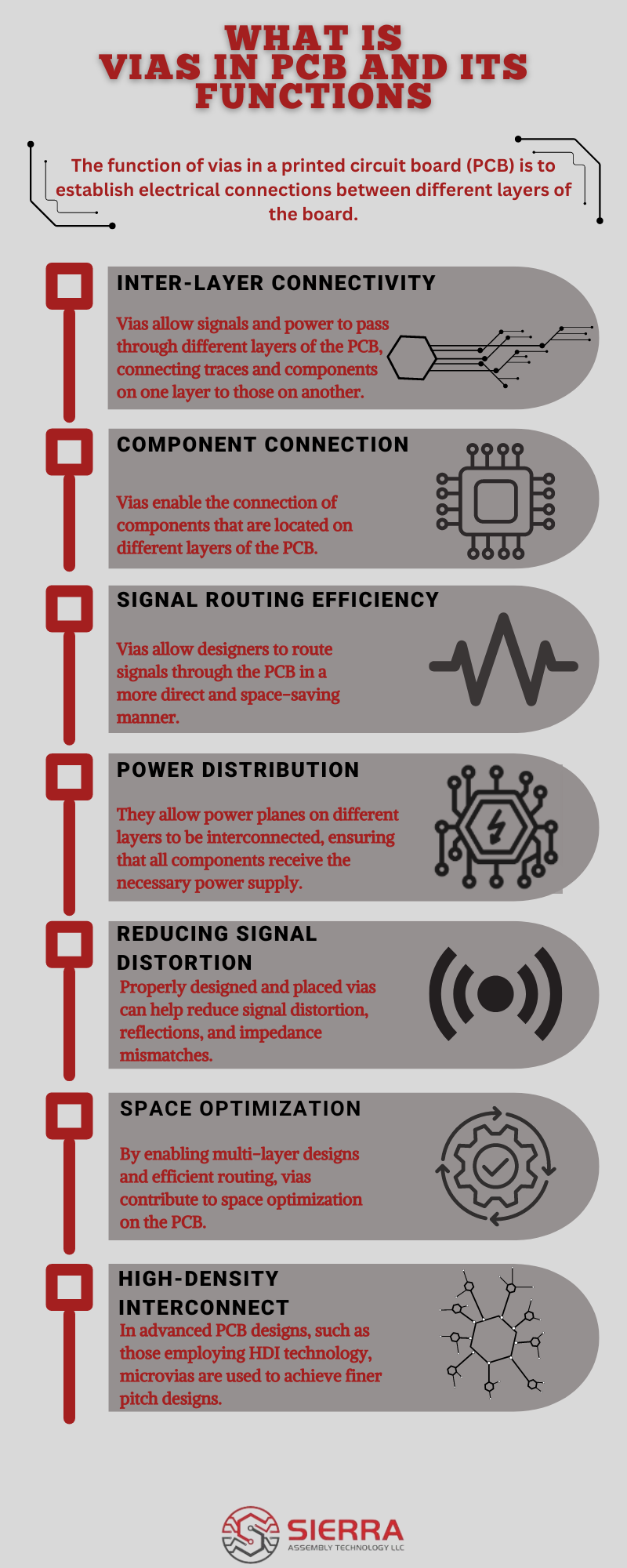
The function of vias in a printed circuit board (PCB) is to establish electrical connections between different layers of the board. PCBs often have multiple layers to accommodate a complex network of traces and components. Circuit board Vias provide a pathway for electrical signals and power to flow between these layers, enabling the efficient interconnection of various components and sections of the circuit.
Here are the primary functions of vias in PCBs:
Vias are essential elements in PCB design, serving as conduits for electrical connections between different layers and contributing to the overall efficiency, reliability, and compactness of electronic circuits. Their proper design and placement are critical for ensuring optimal performance in various applications.
Vias play a pivotal role in PCB layout, offering a multitude of benefits that significantly impact the functionality, efficiency, and manufacturability of electronic circuits.
One of the primary advantages is their ability to establish electrical connections between different layers of the PCB. In multi-layer designs, vias enable the seamless flow of signals and power, allowing for the creation of intricate circuits with components distributed across various layers. This three-dimensional routing capability not only optimizes the use of PCB space but also enhances routing flexibility. Printed circuit board vias reduce congestion on surface layers, providing designers with the flexibility to navigate around obstacles and meet specific layout requirements.
Additionally, vias contribute to the achievement of higher interconnection density in advanced designs, particularly with the use of microvias in High-Density Interconnect (HDI) PCBs. They play a crucial role in maintaining signal integrity by minimizing impedance mismatches and signal distortion, making them essential in high-speed and high-frequency applications.
Furthermore, printed circuit board vias facilitate efficient power distribution by connecting power planes on different layers, ensuring all components receive the required power supply.
In terms of manufacturability, properly designed vias adhere to industry standards, reducing the risk of fabrication errors and contributing to a smoother manufacturing process. Altogether, the strategic incorporation of vias in PCB layout leads to cost-effective designs that are space-optimized, reliable, and versatile in meeting the demands of modern electronic applications.
In printed circuit boards (PCBs), there are several types of vias, each serving specific purposes in terms of connectivity and design. Here are some common types of vias:
Description: A via that extends through the entire thickness of the PCB, connecting the top and bottom layers.
Purpose: Provides a complete electrical connection between different layers.
Description: Connects an outer layer to one or more inner layers but doesn't go through the entire board. It stops at one of the inner layers.
Purpose: Reduces the overall via length, saving space on the board.
Description: Connects two or more inner layers without extending to the outer layers. It is entirely contained within the internal structure of the PCB.
Purpose: Allows for more complex multi-layer PCB designs without affecting the external appearance.
Description: Very small diameter vias, often less than 0.15mm (150 microns) in diameter.
Purpose: Used in high-density interconnect (HDI) PCBs to achieve finer pitch designs and enable miniaturization.
Description: The via is placed directly within a component's landing pad on the surface layer.
Purpose: Helps reduce the pad size and improve routing density, commonly used in high-density designs.
Description: The via is filled with a conductive or non-conductive material after plating.
Purpose: Enhances the reliability and planarity of the PCB surface, often used in advanced technologies.
Description: The via is covered with solder mask on the PCB surface, protecting it from environmental exposure.
Purpose: Prevents solder from wicking into the via during assembly.
Description: The via is capped with a conductive or non-conductive material after plating.
Purpose: Improves the reliability and planarity of the PCB surface, similar to filled vias.
Description: Multiple vias stacked on top of each other.
Purpose: Used when additional routing channels are needed in a limited space.
Description: After the PCB is fabricated, a portion of the via is removed from the opposite side.
Purpose: Reduces signal reflections and improves signal integrity in high-speed designs.
The choice of via type depends on the specific requirements of the PCB design, including factors such as layer count, signal integrity, manufacturing capabilities, and space constraints. Each type of PCB via has its advantages and considerations, and designers select the most appropriate types based on the needs of the application.
The design and placement of vias are crucial considerations in PCB layout, impacting signal integrity, manufacturability, and overall performance. Vias are a key element that allows designers to create intricate, multi-layered circuits that power modern electronic devices.