Solder-related issues remain one of the most common challenges in modern PCB assembly. Among these issues, the solder ball defect is especially important because it can directly affect electrical reliability, product quality, and long-term circuit board performance. Whether in automated SMT production or manual soldering applications, solder balls can lead to shorts, weak connections, and costly rework if not properly controlled.
In electronics manufacturing, even small PCB soldering defects can create major reliability concerns. Solder balls after reflow are commonly found around chip components, IC leads, connectors, and fine-pitch assemblies. These tiny spheres of solder may appear harmless, but they often indicate underlying process problems during stencil printing, solder paste deposition, or the reflow soldering process.
What Is a Solder Ball Defect?
A solder ball defect occurs when small spherical solder particles separate from the main solder joint during PCB assembly. This solder balls commonly form during reflow, wave, or hand soldering processes and can create electrical shorts, reliability issues, and other PCB soldering defects if not properly controlled.
Common solder ball causes during reflow include:
The following table highlights the most common solder ball causes, their impact on PCB assembly reliability, and recommended process solutions used in SMT manufacturing.
|
Common Issue |
Main Cause |
Impact on PCB Assembly |
Recommended Solution |
|
Excessive Solder Paste
|
Too much solder paste deposited on pads
|
Solder balls after reflow and bridging defects
|
Optimize stencil thickness and solder paste volume
|
|
Improper Reflow Profile
|
Rapid heating or incorrect cooling rates
|
Reflow soldering defects and solder splatter
|
Use controlled ramp-up and cooling profiles
|
|
Moisture Contamination
|
Humidity absorbed by PCB or solder paste
|
Solder ball defect formation during reflow
|
Store materials in dry, controlled environments
|
|
Dirty PCB Surface
|
Dust, oil, or oxidation on pads
|
Poor solder wetting and PCB soldering defects
|
Clean PCB surfaces before assembly
|
|
Poor Stencil Alignment
|
Misaligned stencil apertures
|
Uneven solder paste deposition
|
Regular stencil inspection and alignment checks
|
|
Inadequate Solder Mask Design
|
Insufficient spacing between pads
|
PCB solder bridge and electrical shorts
|
Improve solder mask coverage and pad spacing
|
|
Excessive Hand Soldering Temperature
|
Overheating during manual soldering
|
Solder splatter and weak solder joints
|
Maintain proper soldering iron temperature
|
|
Low-Quality Solder Paste
|
Oxidized or contaminated solder materials
|
Increased solder ball causes and poor reliability
|
Use high-quality SMT solder paste
|
|
Component Misalignment
|
Incorrect component placement
|
Solder bridge PCB defects and poor connections
|
Improve pick-and-place accuracy
|
|
Lack of Process Control
|
Inconsistent assembly procedures
|
Multiple PCB soldering defects
|
Implement AOI inspection and process monitoring
|
What Causes Solder Balls During Hand Soldering?
Manufacturers and technicians also frequently ask what causes solder balls during hand soldering, especially during PCB repair or low-volume assembly operations.
Several factors can contribute to solder balls during manual soldering:
-
Excessive solder wire application
-
Poor flux control
-
Oxidized soldering iron tips
-
Incorrect soldering temperature
-
Contaminated PCB surfaces
-
Rapid tip movement causing solder splatter
Hand soldering defects are especially common when operators use inconsistent heating techniques or low-quality solder materials. Proper operator training and controlled soldering temperatures are critical for minimizing these PCB soldering defects.
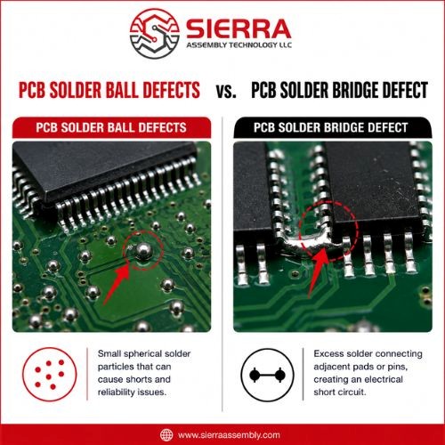
Difference Between Solder Ball Defects and PCB Solder Bridge Issues
Although they are sometimes confused, solder balls and PCB solder bridge defects are different assembly problems.
A solder bridge PCB defect occurs when molten solder unintentionally connects two adjacent pads, leads, or conductors. This creates a direct electrical short circuit between connections.
Solder balls, however, are isolated spherical solder particles that may not immediately create failures but can become reliability risks if they move during operation or thermal cycling.
Comparison Between Solder Ball Defects and PCB Solder Bridges
|
Feature
|
Solder Ball Defect
|
PCB Solder Bridge Defect
|
|
Definition
|
Small isolated solder particles formed during soldering
|
Unwanted solder connection between adjacent conductors
|
|
Electrical Impact
|
May create intermittent shorts
|
Creates immediate short circuits
|
|
Common Cause
|
Excess solder paste, moisture, poor reflow profile
|
Excess solder, poor pad spacing, stencil misalignment
|
|
Typical Location
|
Around ICs, chip components, and connectors
|
Between fine-pitch pads and IC leads
|
|
Reliability Risk
|
Moderate to high over time
|
High and immediate
|
|
Inspection Method
|
AOI, X-ray, visual inspection
|
AOI, electrical testing, visual inspection
|
|
Prevention Method
|
Controlled reflow profile and clean surfaces
|
Accurate solder pastes control and pad spacing
|
Both solder bridge PCB defects and solder ball defects can negatively affect long-term electronic reliability and should be addressed during PCB assembly inspection.
How Solder Balls Affect PCB Reliability
Even small solder balls can create major performance issues in electronic assemblies.
Potential reliability concerns include:
-
Electrical short circuits
-
Signal integrity problems
-
Reduced insulation resistance
-
Intermittent failures
-
Thermal reliability issues
-
Increased rework and repair costs
For industries such as aerospace, medical electronics, automotive systems, and industrial controls, minimizing reflow soldering defects is essential for product reliability and IPC compliance.
Best Practices for Reducing Reflow Soldering Defects
Manufacturers focused on reducing reflow soldering defects should establish consistent process monitoring and inspection procedures.
Key best practices include:
-
Regular stencil cleaning
-
Controlled solder paste storage
-
Periodic reflow oven calibration
-
IPC-compliant process validation
-
Operator training programs
-
Routine solderability testing
-
Continuous quality inspection
Consistent process control is essential for minimizing solder ball defects and improving long-term PCB assembly reliability.
Conclusion
Solder ball defects remain one of the most common PCB soldering defects in SMT assembly and reflow soldering processes. Proper solder paste control, optimized reflow profiles, clean manufacturing environments, and consistent inspection procedures are essential for minimizing solder balls after reflow and improving long-term PCB reliability. With proper process control and quality assurance practices, manufacturers can significantly reduce solder-related defects and improve electronic assembly performance.
Frequently Asked Questions
1. What causes solder balls during reflow soldering?
Ans: Solder balls during reflow are commonly caused by excessive solder paste, moisture contamination, rapid heating rates, poor stencil alignment, or unstable solder paste behavior.
2. Are solder balls considered PCB defects?
Ans: Yes. Excessive solder balls are considered PCB soldering defects because they can reduce electrical reliability and increase the risk of short circuits.
3. What causes solder balls during hand soldering?
Ans: Common causes include excessive solder application, incorrect soldering temperature, poor flux control, oxidized soldering tips, and contaminated PCB surfaces.
4. What is the difference between solder balls and solder bridges?
Ans: Solder balls are isolated solder particles, while a solder bridge PCB defect occurs when solder connects adjacent conductors and creates a direct electrical short.
5. Can solder balls cause PCB failure?
Ans: Yes. Loose solder balls may shift during vibration or thermal cycling and create intermittent electrical shorts or reliability failures.
6. How can manufacturers prevent solder balls after reflow?
Ans: Manufacturers can reduce solder balls after reflow by optimizing solder paste application, controlling reflow profiles, maintaining clean PCB surfaces, and implementing AOI inspection systems.
7. What is PCB solder bridge defect?
Ans: A PCB solder bridge defect happens when excess solder connects two nearby pads or pins, creating an unintended electrical short circuit on the PCB.
Partner With Sierra Assembly Technology for Reliable PCB Assembly Solutions
Reducing solder ball defects and improving long-term PCB reliability requires more than just quality materials. It also depends on working with an experienced PCB assembly partner that understands SMT process control, reflow soldering optimization, inspection standards, and manufacturing consistency.
At Sierra Assembly Technology, we provide high-quality PCB assembly solutions designed to support complex electronic manufacturing requirements across aerospace, medical, industrial, automotive, and telecommunications industries.
Our team focuses on precision SMT assembly, advanced inspection processes, controlled manufacturing environments, and strict quality standards to help minimize PCB soldering defects and improve overall product reliability.
Our PCB assembly capabilities include:
-
SMT and through-hole PCB assembly
-
Prototype and low-volume production
-
Reflow soldering process optimization
-
X-ray inspection services
-
Functional testing and quality verification
-
Lead-free and RoHS-compliant manufacturing
-
Quick-turn PCB assembly support
Whether you need support with prototype PCB assembly, process optimization, or high-reliability electronics manufacturing, Sierra Assembly Technology is committed to delivering dependable PCB assembly services with consistent quality and fast turnaround times.
Contact our team today to learn how our PCB assembly solutions can support your next electronics manufacturing project.
Related Blogs

