PCBs are at the heart of the modern technological landscape, powering electronic devices and systems that have become indispensable in our daily lives. Their importance extends to advancements in technology, efficient manufacturing processes, customization options, and the continuous evolution of electronics to meet the demands of an increasingly connected and tech-driven world.
PCBs are the foundation of almost all electronic devices we use daily, including smartphones, laptops, tablets, televisions, cameras, smartwatches, and more. These devices rely on PCBs to connect and power the electronic components that make them function.
Using quality
materials in PCB design is vital for achieving a high level of reliability, performance, and functionality. It ensures that the PCB meets design specifications, operates consistently over time, and withstands various environmental and mechanical challenges.
Understand the Whys Behind PCB Failure and Troubleshooting
PCB failure refers to the condition when a Printed Circuit Board (PCB) experiences a malfunction or ceases to operate as intended. PCB failure can occur due to various factors, and it can lead to the non-functioning of the electronic device or system where the PCB is employed. PCB failure can manifest in different ways, depending on the cause and the severity of the issue.
Common Causes of PCB Failure Modes
Circuit board diagnostics play a critical role in identifying the root cause of PCB failure. When a PCB experiences malfunctions or non-functioning, diagnostic procedures are used to pinpoint the faulty components or areas of the board. PCB (Printed Circuit Board) failure can occur due to various reasons, and these failures can be categorized into different modes based on the underlying cause.
-
Soldering Defects: Poor soldering of components onto the PCB, such as cold solder joints or solder bridges, can lead to connectivity issues and intermittent failures.
-
Component Failure: Electronic components, such as resistors, capacitors, and integrated circuits, can fail due to manufacturing defects, aging, or external factors like voltage spikes or overheating.
-
Environmental Factors: Exposure to harsh environmental conditions, such as high temperature, humidity, dust, or corrosive substances, can cause PCB materials to degrade or electronic components to malfunction.
-
Mechanical Stress: Physical stress, such as bending, vibration, or shock, can cause mechanical failure of solder joints or fractures in the PCB, leading to connectivity problems.
-
Electrical Overload: PCBs can fail if they are subjected to excessive electrical current or voltage beyond their design limits, causing burnouts or damage to electronic components.
-
Design Errors: Inadequate PCB design, including incorrect trace routing, inadequate trace widths, or insufficient clearance between traces, can lead to performance issues or short circuits.
-
EMI/EMC Interference: Electromagnetic interference (EMI) or electromagnetic compatibility (EMC) issues can cause signal interference and lead to erratic behavior or malfunctions.
PCB troubleshooting often requires a process of elimination and
various testing methods, such as visual inspection, electrical testing, thermal testing, and X-ray analysis. Once the cause of the failure is identified, the PCB can be repaired or replaced to restore its functionality.
Impact of PCB Failure on Industries
PCB (Printed Circuit Board) failure can have significant impacts on industries, affecting various aspects of operations, productivity, and financial performance. Some of the key impacts of PCB failure on industries include:
-
Downtime and Production Loss: PCB failures in critical industrial systems can lead to unplanned downtime, halting production processes. This results in decreased productivity and revenue loss for the company.
-
Increased Maintenance and Repair Costs: PCB failures require repairs or replacements, which can be costly, especially if the PCBs are complex or require specialized components. The increased maintenance costs can affect the profitability of industries.
-
Supply Chain Disruptions: If PCB failures affect critical components or systems in the supply chain, it can cause disruptions and delays in product deliveries, impacting overall supply chain efficiency.
-
Product Recalls and Reputational Damage: In industries where PCB failures pose safety risks or affect a large number of products, manufacturers may need to initiate costly product recalls. This can lead to reputational damage and loss of consumer trust.
-
Waste and Environmental Impact: Failed PCBs can contribute to electronic waste (e-waste) if not properly recycled or disposed of. Improper e-waste management can have adverse environmental consequences.
-
Reduced Reliability and Safety Concerns: Industries that rely on electronic systems with PCB failures may face concerns about the reliability and safety of their products or processes. This can lead to decreased customer confidence and potential liability issues.
-
Competitive Disadvantage: Industries that experience frequent PCB failures may face a competitive disadvantage compared to competitors with more reliable products and systems.
-
Decreased Operational Efficiency: PCB failures can disrupt operations and workflows, leading to decreased operational efficiency and increased lead times for completing tasks.
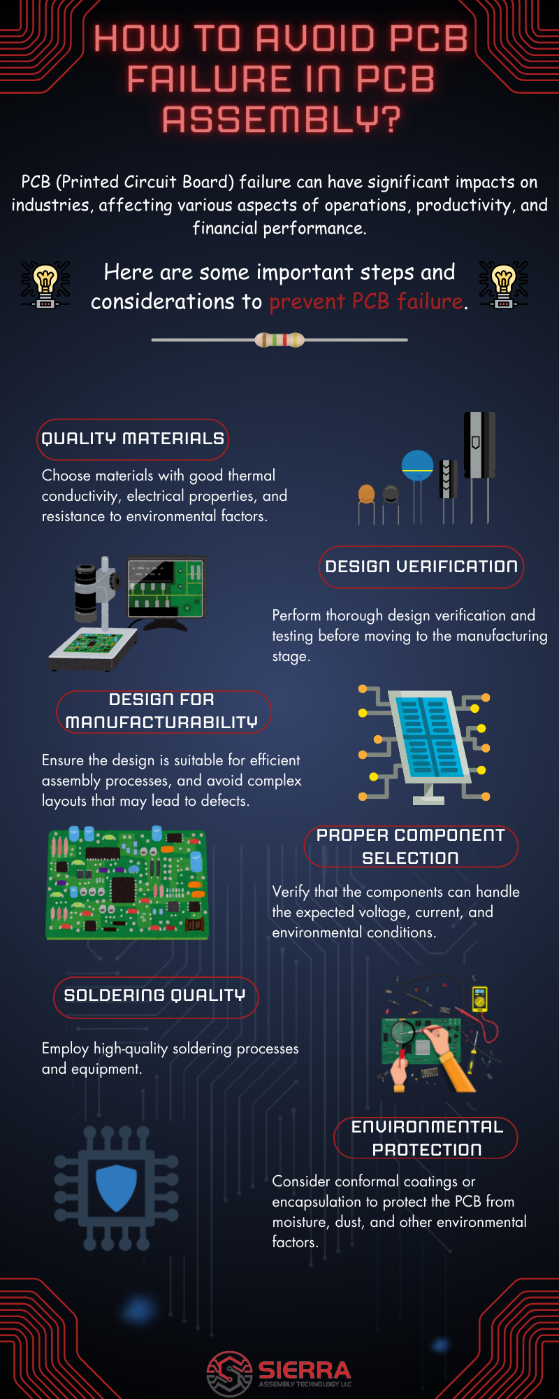
How to Avoid PCB Failure in PCB Assembly?
To avoid PCB failure in
PCB assembly, careful attention should be given to the entire design and manufacturing process. Here are some important steps and considerations to prevent PCB failure:
-
Quality Materials: Use high-quality PCB materials that are appropriate for the application and operating environment. Choose materials with good thermal conductivity, electrical properties, and resistance to environmental factors.
-
Design Verification: Perform thorough design verification and testing before moving to the manufacturing stage. Use simulation tools to check for potential issues like signal integrity problems, thermal hotspots, and clearance violations.
-
Design for Manufacturability (DFM): Design the PCB with manufacturing in mind. Ensure that the design is suitable for efficient assembly processes, and avoid complex layouts that may lead to defects.
-
Proper Component Selection: Choose reliable and suitable components for the application. Verify that the components can handle the expected voltage, current, and environmental conditions.
-
Soldering and Assembly Quality: Employ high-quality soldering processes and equipment. Use automated assembly methods when possible to reduce the risk of human error.
-
Thermal Management: Implement effective thermal management strategies to prevent overheating. Use heat sinks, thermal vias, and proper component placement to dissipate heat efficiently.
-
Environmental Protection: Consider conformal coatings or encapsulation to protect the PCB from moisture, dust, and other environmental factors.
-
Electromagnetic Compatibility (EMC): Ensure that the PCB design meets electromagnetic compatibility standards to minimize the risk of interference and signal disruptions.
-
Testing and Inspection: Conduct thorough testing and inspection at various stages of the manufacturing process. This includes in-circuit testing (ICT), functional testing, and visual inspection.
-
Component Handling and Storage: Properly handle and store components to prevent damage from electrostatic discharge (ESD) or exposure to environmental hazards.
-
Corrective Actions: Analyze any previous failures or defects to identify root causes and implement corrective actions to prevent similar issues in the future.
-
Prototyping and Iterative Improvement: Prototype the PCB design and test it in real-world conditions before full-scale production. Use iterative improvement to fine-tune the design and address any issues that arise during prototyping.
-
Regular Maintenance and Monitoring: For deployed systems, implement regular maintenance and monitoring procedures to detect and address potential issues before they lead to failure.
By following these practices, PCB assemblers can significantly reduce the likelihood of PCB failure, diagnostics and ensure that electronic devices and systems operate reliably and efficiently over their intended lifespans.
Related Blogs

