A Discussion on Various PCB Testing Techniques

Modern PCB Testing Techniques Explained: ICT, FCT, Flying Probe, JTAG & Reliability Methods for 2024–25

Dec 25,2025


PCB Testing Techniques

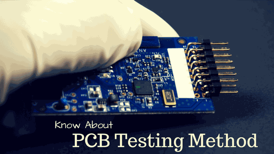
Ensuring high-quality PCB performance requires advanced testing methods that validate electrical functionality, component accuracy, and long-term reliability. As PCBs become smaller and more complex, manufacturers now rely on multiple testing techniques to identify defects early and improve product reliability

What Is PCB Testing?

PCB testing is the process of verifying that a printed circuit board assembly (PCBA) performs correctly before it is integrated into a final product.
It helps identify issues such as:
  • Shorts and open circuits
  • Incorrect component placement
  • Soldering defects
  • Electrical value mismatches
  • Firmware or interface failures
  • Reliability and contamination issues
PCB Testing Methods

Testing Method

What It Does

When It’s Used

In-Circuit Testing (ICT)

Verifies components, shorts/opens, electrical values

Medium–high volume production

Functional Testing (FCT)

Tests a board under real operating conditions

Final validation stage

Flying Probe Testing (FPT)

Checks basic electrical performance without a fixture

Prototypes & small batches

Boundary Scan (JTAG)

Tests IC pins, interconnects, BGAs

High-density digital PCBs

Micro-Section Analysis

Examines internal layers & solder joints

Root cause / failure analysis

Optical Microscopy

Detects surface defects and solder issues

Quality control inspections

Burn-In Testing

Identifies early-life component failures

High-reliability applications

Contamination Testing

Measures ionic residue & impurities

High-voltage & high-frequency designs

1. In-Circuit Testing (ICT)

In Circuit Testing (ICT) is one of the most accurate PCB testing techniques for verifying individual components on an assembled board.

What In-Circuit Testing checks

  • Shorts & open circuits
  • Resistance, capacitance, inductance
  • Diode/transistor functionality
  • Component orientation
  • Solder joint integrity

Why manufacturers use of In Circuit Testing

  • Fast and automated
  • Ideal for large production runs
  • Detects component-level defects early

2. Functional Circuit Testing (FCT)

Functional Testing simulates real-world conditions the PCBA will face once deployed.

Functional Circuit Testing validates

  • Power sequence and voltage behavior
  • Input/output operations
  • Firmware interactions
  • Performance under load

When Functional Circuitis used

  • Final stage of PCB testing
  • Before integration into the final product
  • For devices requiring real-time performance validation

3. Flying Probe Testing (Fixtureless ICT)

Flying Probe Testing (FPT) uses moving probes instead of a dedicated fixture.

Key features of Flying Probe Testing

  • No fixture cost → ideal for prototypes
  • Quick program setup
  • Supports design changes easily

Flying Probe Testing checks

  • Opens & shorts
  • Passive component values
  • Polarity
  • Basic functional behavior

Comparison: ICT vs Flying Probe

Feature

ICT

Flying Probe

Fixture Required

Yes

No

Speed

Very fast

Slower

Best For

Mass production

Prototypes / low volume

Cost

High setup cost

Lower cost

Accuracy

Very high

Moderate–high


4. Boundary Scan (JTAG Testing)
Boundary Scan Testing is used especially for high-density digital boards where test access is limited.

What it tests

  • IC interconnects
  • BGA connections
  • Pin logic states
  • High-speed digital signals

Advantages of JTAG Testing

  • No physical probe access required
  • Implements IEEE 1149.1 standard
  • Great for SoCs, FPGAs, microcontrollers
5. Optical Microscopy Testing

Used for visual inspection of surface defects.

Checks for Optical Microscopy Testing

  • Solder cracks
  • Misalignment
  • Delamination
  • Bent leads
6. Micro-Section / Cross-Section Analysis

A 2D section of PCB is removed to analyze internal structures.

Micro-Section of Used to identify Analysis 

  • Via/trace failures
  • Plating cracks
  • Solder voids
  • Copper thickness
  • Delamination

Micro Section Common Analysis

  • Failure analysis
  • Quality audits
  • Certification/testing labs

7. Burn-In Testing

This reliability test exposes boards to elevated temperatures and voltages.

Purpose of Bur-in Testing

  • Detect early-life component failures
  • Validate performance under stress
  • Identify weak or unstable components
Widely used in aerospace, automotive, medical, and industrial electronics.

8. PCB Contamination / Ionic Cleanliness Testing

Ensures the PCB is free from harmful ionic residues.

Sources of contamination Testing

  • Flux residue
  • Fingerprints
  • Chemicals
  • Moisture absorption

Sources of contamination -Why it matters

  • Corrosion
  • Leakage currents
  • High-voltage failures
This test is essential for long-term reliability.

Frequently Asked Questions

1. What is the most common PCB testing method used in electronics manufacturing?

Answer: The two most commonly used PCB testing methods are In-Circuit Testing (ICT) and Functional Circuit Testing (FCT). ICT checks component placement, shorts/opens, and electrical values. FCT verifies that the PCB functions correctly under real operating conditions. Manufacturers typically use both methods to ensure component-level and system-level accuracy.

2. What is the difference between ICT and Flying Probe Testing?

Answer: The biggest difference is fixture requirement and cost: ICT needs a custom fixture, making it ideal for mass production because it’s fast and highly accurate, Flying Probe Testing does not require a fixture, making it perfect for prototypes, engineering builds, and low-volume production.ICT is faster and more precise, while Flying Probe is more flexible and cost-efficient during early design stages.

3. How does Functional Circuit Testing (FCT) work in PCB assembly?

Answer: FCT simulates real-world operating conditions to verify the performance of the assembled PCB. During testing: Power is applied to the board, Inputs and outputs are monitored. Firmware and communication interfaces are validated. FCT ensures the PCBA behaves correctly before being installed in the final product.

4. Why is Boundary Scan (JTAG) testing important for high-density PCBs?

Answer: Boundary scan testing is essential for boards with BGAs, fine-pitch ICs, and dense layouts where physical access is limited. Using the IEEE 1149.1 standard, JTAG allows engineers to: Test internal IC pins, Verify digital interconnects, Detect BGA solder faults. It provides excellent coverage without requiring probes or physical access.

5. How do manufacturers check PCB reliability during testing?

Answer: Manufacturers use reliability tests like: Burn-In Testing: Exposes the board to high temperature and voltage to detect early failures. Thermal cycling: Tests durability under repeated temperature changes. Ionic contamination testing: Ensures no corrosive residues remain. These tests make sure the PCB can withstand long-term field use without performance issues.

Related Blogs