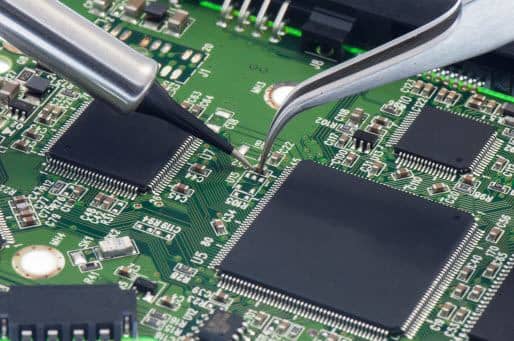
Minimizing defects is a top priority for electronics manufacturers across the United States. Whether serving aerospace, medical, industrial, or consumer markets, understanding common PCB assembly issues is essential to ensuring product reliability and performance.
As circuit designs become more compact and complex, the risk of PCB assembly defects increases. Without proper controls, these issues can lead to functional failures, costly rework, or complete product rejection.
This guide explains the most common PCB manufacturing problems, their root causes, and proven prevention methods. Learn more
about our PCB assembly services to see how we ensure high-quality production and defect prevention
Why PCB Assembly Issues Matter
Even minor printed circuit board assembly issues can cause:
-
Electrical shorts
-
Signal interference
-
Reduced product lifespan
-
Regulatory non-compliance
Preventing
PCB failure causes begins with proper design, fabrication, and inspection.
6 Common PCB Assembly Issues and How to Prevent Them
1. Solder Bridging
Solder bridging in PCB occurs when solder unintentionally connects adjacent pads or traces, creating electrical shorts.
|
Causes |
Prevention |
|
Excess solder paste |
Use proper solder mask design |
|
Poor stencil alignment |
Ensure stencil-to-board alignment |
|
Tight pad spacing |
Perform automated optical inspection (AOI) |
2. Plating Voids
Plating voids in PCB are gaps in copper plating inside plated through-holes, disrupting electrical continuity.
|
Causes |
Prevention |
|
Contaminated drilling debris |
Thorough pre-plating cleaning |
|
Air bubbles during copper deposition |
Controlled electroplating processes |
|
Poor hole cleaning |
Strict PCB quality control |
Controlled electroplating processes and thorough hole cleaning are essential. Explore
PCB fabrication quality controls
to minimize plating voids in production.
3. Non-Wetting Solder Joints
Non-wetting solder joints occur when solder fails to properly adhere to copper pads, resulting in weak connections.
|
Causes |
Prevention |
|
Oxidized PCB surfaces |
Proper humidity-controlled storage |
|
Improper storage conditions |
Use of fresh, protected PCBs |
|
Contaminated solder materials |
Controlled soldering temperatures |
4. Acid Traps
PCB acid traps form when sharp angles in trace layouts trap chemical residues during fabrication.
|
Causes |
Prevention |
|
Poor PCB design geometry |
Avoid sharp angles in layouts |
|
Acute trace angles |
Apply solder mask or epoxy to vulnerable areas |
|
Tight pad spacing |
Follow design-for-manufacturability (DFM) guidelines |
5. Physical Damage
Physical damage in PCB is often invisible but can severely impact performance.
|
Causes |
Prevention |
|
Dropping boards during prototyping |
Use ESD-safe handling procedures |
|
Improper handling during SMT assembly |
Proper packaging and transport |
|
Environmental stress |
Trained personnel during assembly |
6. Electromagnetic Interference (EMI)
Electromagnetic interference PCB issues affect signal integrity and system reliability.
|
Causes |
Prevention |
|
Inadequate grounding |
Increase ground plane coverage |
|
Poor trace routing |
Optimize PCB layout design |
|
Insufficient shielding |
Perform EMI testing during validation |
PCB Issues and Prevention
|
PCB Issue |
Primary Cause |
Prevention Method |
|
Solder Bridging |
Excess solder |
AOI & stencil control |
|
Plating Voids |
Contamination |
Clean drilling & plating |
|
Non-Wetting |
Oxidation |
Controlled storage |
|
Acid Traps |
Design flaws |
Improved layout geometry |
|
Physical Damage |
Mishandling |
ESD & handling protocols |
|
EMI Issues |
Poor grounding |
Layout optimization |
Effective PCB assembly inspection includes:
-
Automated optical inspection (AOI)
-
X-ray inspection for hidden joints
-
Electrical testing
These steps are essential for maintaining
high-quality PCB assembly. Effective inspection is critical to reduce defects. Check our
PCB assembly inspection services for advanced quality control solutions.
Why Work with Professional PCB Assembly Services?
Expert
PCB assembly services ensure:
-
Reduced defects
-
Compliance with industry standards
-
Reliable, long-term performance
Frequently Asked Questions (FAQ)
1. What is the most common PCB soldering defects and how can they be avoided?
Answer: Common PCB soldering defects include cold joints, solder bridging, and non-wetting solder joints. They can be prevented by controlling solder paste application, maintaining proper reflow temperatures, and ensuring PCBs are stored in humidity-controlled environments.
2. How does electromagnetic interference in PCB affect performance?
Answer: Electromagnetic interference (EMI) can cause signal distortion, cross-talk, or complete circuit failure. Reducing EMI involves proper PCB layout, increasing ground plane coverage, using shielding techniques, and following best design-for-manufacturability (DFM) practices.
3. Why is PCB defect prevention important for electronics manufacturers?
Answer: PCB defect prevention helps minimize costly rework, product recalls, and functional failures. By implementing strict quality control, automated inspection, and proper assembly processes, manufacturers can ensure reliable and long-lasting products.
4. What role does PCB quality control play in reducing assembly errors?
Answer: PCB quality control identifies issues such as plating voids, acid traps, and misaligned components before final assembly. It includes automated optical inspection (AOI), X-ray inspection, and electrical testing, which together reduce PCB assembly errors and improve product reliability.
5. How do professional PCB assembly services help prevent printed circuit board assembly issues?
Answer: Professional PCB assembly services offer expertise in design review, soldering processes, inspection, and testing. Their experience ensures that printed circuit board assembly issues like misalignment, solder defects, and EMI problems are minimized, leading to high-quality PCB assembly and improved production yield.
Conclusion
Managing common PCB assembly issues is essential for reducing PCB assembly defects and avoiding costly PCB manufacturing problems. By following proper design practices, maintaining strong PCB quality control, and conducting effective PCB assembly inspection, manufacturers can
ensure high-quality PCB assembly and long-term product reliability. Partnering with experienced PCB assembly services further supports consistent performance and defect prevention. Partnering with experienced PCB assembly services supports consistent performance and defect prevention.
Contact our PCB assembly experts to discuss your project needs.
Related Blogs

