Subscribe to get the latest news and updates. No span, we promise.

|
Feature |
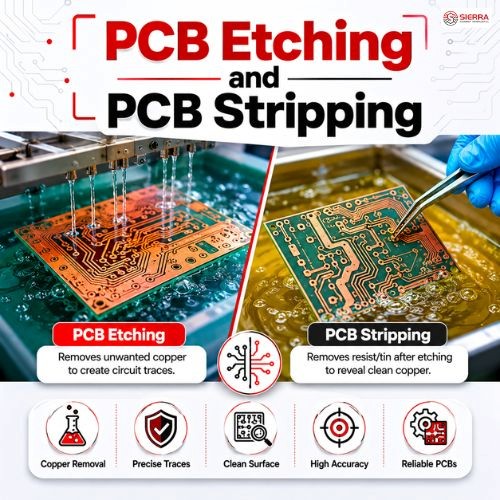
PCB Etching |
PCB Stripping |
|
Main Purpose |
Removes unwanted copper |
Removes protective coatings |
|
Manufacturing Stage |
Circuit formation stage |
Post-etch cleaning stage |
|
Material Removed |
Copper |
Photoresist or tin |
|
Importance |
Creates electrical traces |
Prepares PCB for finishing |
|
Common Methods |
Chemical, laser, plasma |
Chemical, plasma, dry film |
|
PCB Etching Defect |
Main Cause |
Impact on PCB |
|
Over-Etching |
Excessive chemical exposure |
Damaged or narrow copper traces |
|
Under-Etching |
Incomplete copper removal |
Electrical short circuits |
|
Uneven Copper Traces |
Poor chemistry balance |
Inconsistent signal performance |
|
Residue Buildup |
Inadequate cleaning process |
Reduced solderability |
|
Poor Line Definition |
Weak process accuracy |
Lower circuit precision |