Subscribe to get the latest news and updates. No span, we promise.

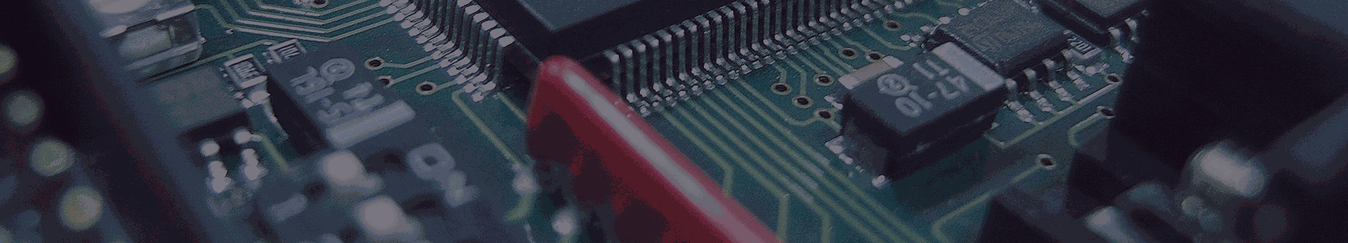
Compact and high-density electronic devices are becoming the norm in aerospace, automotive, medical, and consumer electronics industries in the U.S. With miniaturization comes complexity in PCB assembly. One of the most common quality issues faced during assembly is pcb warpage, also called board warpage.
Simply put, warpage in PCB occurs when a printed circuit board bends or twists due to stress during manufacturing or assembly. Even slight warping can result in defective solder joints, poor component placement, and operational failure in high-density assemblies.
A proactive approach is required to prevent pcb warpage issues, as this ensures that your assembly meets quality standards and reliability expectations.
|
Cause |
Explanation |
|
PCB Design |
Unbalanced layers, misaligned fibers, or unequal copper distribution can lead to upward or downward bending of the board. |
|
Thermal Expansion |
Improper heating during soldering or reflow causes copper layers to expand differently, creating stress and warping. |
|
Panelization Issues |
Uneven copper densities in outrigger areas or improper tab sizes during depanelization may distort the board. |
|
Thicker PCBs |
High-layer or thick PCBs may retain stress if layers aren’t properly distressed, causing bending post-assembly. |
Other factors include: inconsistent laminate materials, excessive moisture content, and improper reflow profiles. These all contribute to pcb warpage issues that can compromise assembly quality.
Maintaining PCB integrity requires adherence to standards. PCB warpage specifications guide engineers to acceptable limits, ensuring operational reliability:
|
Parameter |
Recommended Value |
|
Maximum Warpage |
≤ 0.75% of PCB diagonal |
|
Allowable Bow |
≤ 0.5 mm |
|
Twist |
≤ 0.5° |
These pcb warpage specs may vary based on the application, such as aerospace, automotive, or consumer electronics. Measuring warpage accurately is critical to avoid pcb warpage issues during assembly.
Accurate measurement helps detect potential defects before assembly:
Tracking pcb warpage measurement ensures compliance with pcb warpage standards, prevents assembly defects, and enhances yield.
Preventing warpage in PCB assembly is possible through design and assembly adjustments:
|
Design Adjustment |
Impact on PCB Warpage |
|
Balanced Copper Weight |
Reduces thermal expansion mismatch across layers. |
|
Optimized Thermal Profiles |
Prevents excessive heating and stress during reflow soldering. |
|
Minimized Edge Clearance |
Reduces stress points along pallet and fixture contact areas. |
|
Baking PCB Above Tg |
Relieves internal stress and stabilizes high-layer boards. |
By incorporating these pcb warpage prevention measures, designers can significantly reduce pcb warpage issues and improve reliability.
Background:
A leading U.S.-based automotive electronics company was designing a multi-layer PCB for an advanced driver-assistance system (ADAS). The board had over 900 components with a mix of SMT and through-hole placements. Initial assemblies showed pcb warpage, resulting in:
Challenges:
|
Issue |
Cause |
Impact |
|
PCB bending |
Unbalanced copper layers |
Solder defects during reflow |
|
Misalignment |
Excessive thermal stress |
Defective placement of sensors |
|
Panelization distortion |
Large tabs & outriggers |
Depanelization errors |
Results:
|
Metric |
Before Sierra |
After Sierra |
|
Warpage Incidents |
18% |
2% |
|
Solder Defects |
High |
Reduced by 85% |
|
Assembly Rework |
Frequent |
Minimal |
|
Compliance |
Partial |
Met Automotive Standards |
This pcb warpage case study highlights how preventive measures during design and assembly can save time, cost, and improve product reliability.
At Sierra Assembly, we combine advanced PCB design practices with assembly expertise:
Our approach ensures every board meets high U.S. standards and performs reliably in demanding applications.
1. What is PCB Warpage and How Does It Affect Assembly?
Answer: PCB warpage is bending or twisting of a board during manufacturing. It can cause solder defects, misaligned components, and assembly failures.
2. What Are the Main Causes of Warpage in PCB Assembly?
Answer: Unbalanced layers, thermal expansion, panelization issues, thick PCBs, moisture, and poor reflow profiles.
3. How Can PCB Warpage Be Measured Accurately?
Answer: Mechanical gauges, laser scanning (3D mapping), and optical profilometry (non-contact high-res measurement).
4. What Design Changes Can Prevent PCB Warpage?
Answer: Balance copper layers, optimize thermal profiles, minimize edge clearance, bake above Tg, and verify panelization.
5. Why Is Preventing PCB Warpage Critical for Automotive and Aerospace?
Answer: It ensures solder reliability, component alignment, compliance with standards, higher yield, and cost savings.
PCB warpage is a critical challenge in modern high-density electronics. Understanding the causes like thermal stress, unbalanced layers, and panelization issues and implementing prevention measures is essential to maintain quality and reliability.
With proper design adjustments, measurement techniques, and a reliable assembly partner like Sierra Assembly, you can prevent pcb warpage issues, adhere to pcb warpage standards, and produce high-quality boards for automotive, aerospace, and industrial applications.
A proactive approach to pcb warpage measurement, specification compliance, and preventive design ensures that your products perform flawlessly in the field, saving time, cost, and reputational risks.