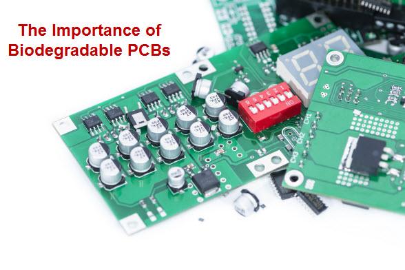
Electronic devices are meant to make our lives simpler. However, the threat they bring to the environment is massive and beyond the control now! Unlike the past, electronic devices are manufactured with reduced shelf life, and within a few years of usage, they are being thrown away. As a result of this, there has been a huge increase in the volumes of e-waste that are generated and disposed of carelessly to the environment. Although the local, state and national authorities are taking efforts to recycle this e-waste, they fail to reach the expected level of speed mainly due to the difficulty in recycling or decomposing the PCBs used in the gadgets. According to several studies, the PCBs in the boards largely contribute to the release of toxic substances to the environments such as mercury, cadmium and lead, among others. Considering this, todays’ PCB manufacturers strive to assemble and manufacture boards that are biodegradable. How are these biodegradable PCBs made and how would they contribute to environmental sustainability? Read on the post to know more!

The Making of Biodegradable Boards
To cop up with the increasing rate of e-waste generation caused mainly due to PCBs of various shapes and sizes, researchers and scientists have devised the idea of biodegradable boards. The main advantage of these boards is that, it is assembled and manufactured in such a way to completely disintegrate when exposed to water for 10 minutes. Isn’t that interesting? To make that disintegration possible, biodegradable PCBs are assembled and manufactured following the below mentioned steps.
-
Commercial Off-the-Shelf Components (COTS): These are nothing but transistors, sensors, and power supplies that commonly go in the making of even conventional PCB boards. Even in the assembly and manufacturing of biodegradable PCBs, the use of these COTS components is mandatory.
-
Application of Magnesium Paste: During the assembly of biodegradable PCBs, all Commercial Off-the-Shelf Components aforementioned are attached to the top layer of the board utilizing magnesium paste. After the application, the board is exposed to the room temperature, resulting in the creation of a solid adhesive between the components and PCB.
-
Applications of Tungsten Paste: In order to provide connectivity to the top and bottom circuit board layers, via holes are filled with Tungsten Paste.
-
Sodium Carboxymethylcellulose (Na-CMC) Substrates – Several manufacturers utilize (Na-CMC) as a substrate material in the manufacture of biodegradable PCBs. Usually, this substrate material is formed at 50 µm in thickness on the top and bottom layers of the board.
-
Polyethylene Oxide (PEO) Bonding Layer – The Na-CMC substrate layers are bonded together utilizing Polyethylene Oxide (PEO).
Currently, the PCB manufacturers have been trying and testing several other ways to assemble and manufacture completely biodegradable PCBs and partially biodegradable PCBs. The most popular amongst such methods are the ones using bio-composites that are produced from natural cellulose fibers extracted from banana stems and wheat gluten or using chicken feathers and e glass fibers. Whatever are the methods, the practice of building biodegradable PCB boards largely contributes to minimize e-waste, which otherwise has a tragic environmental impact. With several years of experience in
PCB fabrication,
PCB prototyping,
PCB assembling and
PCB rework, leading PCB manufacturers like Sierra Assembly Technologies are looking towards a sustainable future and ensure the widespread assembly and manufacture of biodegradable PCBs.


