A Step Back in Time: History of PCBs

A Step Back in Time: History of PCBs

Oct 22,2015

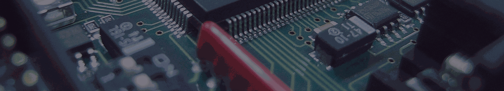
Printed Circuit Boards (PCBs) are used in almost all electronic applications. From mobile phones to aircrafts, almost all of the products used daily are supported by PCBs. Understanding the history of PCBs will help us appreciate the effort that has gone into developing this product as well as the importance they hold today.

1920s – 2000s: History of PCBs

Below is a timeline of the history of PCBs:

  1. 1920s - Radios and gramophones sported this technology in the twenties. The boards were made of wood, Masonite, and other such materials.
  2. 1947 - The first double sided PCB with plated through holes was developed.
  3. 1950s - The first etching pattern of the circuit was introduced. The boards were designed with the wiring on one side and the components on the other.
  4. 1960s - Multilayer PCBs were produced commercially.
  5. 1970s - The Japanese used aqueous developed LPIs (liquid photo imageable masks) for screen processes, making it the global industry standard. The size of the PCBs was smaller as well.
  6. 1980s - Components were surface mounted making the PCB size still smaller.
  7. 1990s - The PCBs being developed were much more economical by this point in time. However, the quality of the product was still the same.
  8. 2000s - The quality of the product increased, while the size reduced considerably. Rigid-flex and flexible PCB options became more affordable.

Going forward, the PCB industry is set to evolve further. Miniaturization is the way to go. As the world of almost every individual is being governed by the use of electronics, PCBs are expected to evolve according to user behavior. The need for lighter, sturdier, and smaller devices has led to miniaturization of PCBs. In the future, there is a possibility of development of embedded components, 3-dimensional boards, integrated circuit chips, along with miniaturization of PCBs.