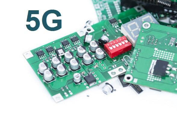
There is too much information on 5G devices, which will be wireless. These devices will have a profound impact on everything right from mobile phones to several wireless devices used in daily lives. 5G devices are expected to have 10X faster data rates than their 4G counterparts, and can easily achieve 100X faster speeds whenever required. With so many advantages to offer, it is quite obvious that these devices will raise technical standards for hardware, as well as printed circuit boards. With broader and faster bandwidth requirements, every PCB will be subjected to high standards of quality and performance. Although PCB manufacturers have already started investing in production processes and manufacturing systems that assure them quality products, there are several challenges to be addressed. What are the top challenges faced by PCB manufacturers eyeing 5G applications? What are the different 5G ready technologies utilized by these manufacturers to overcome these challenges? Read the post to know more.
An Outlook on Manufacturing Challenges Faced by 5G Wireless Printed Circuit Board Manufacturers
For 5G applications, the risk of system failure increases, if the PCB fails to perform. The PCBs may fail, if they are daunted by the following challenges:
-
Signal Integrity: As 4G devices, most 5G devices will require high-density interconnects (HDIs) featuring thinner traces. These thinner traces are used because they help reduce the device size, and are perfect for input/output signals, too. However, these thinner lines may raise signal integrity problems in 5G devices. If the physical characteristics of these lines vary minutely then they may delay the signals by several microseconds, which may affect in the long run.
-
Impedance Anomalies: Strict impedance is one of the important requirements for high-frequency signals. In HDI’s, the impedance may be affected by the cross-section of the line’s shape, dimension, space/line width, as well as several other factors. Additionally, the cross-section created using subtractive etching may produce several impedance anomalies. To address this, nowadays, PCB manufacturers are adopting modified semi-additive processes (mSAP), which help ensure the precision of line traces. These line traces can also be designed with straight walls to assure better impedance control.

Different Technologies Adopted by PCB Manufacturers to become 5G Ready
The following technologies are helping PCB manufacturers to become future-ready for 5G applications.
-
Modified Semi-Additive Process: This is allowing 5G device manufacturers to achieve high density without fearing signal degradation. During the process, the laminate is coated with a thin layer of copper. Being an additive process, this copper lamination is performed in areas, where resist is absent. The copper that is found between the conductors is then etched out. Unlike the earlier subtractive processes, the etch geometries are better chemically defined in this process. This defining is performed using photolithography, which helps ensure a higher precision and minimized signal loss.
-
Advanced Automated Optical Inspection Systems (AOIs): AOIs are not new, and they have been used for a long time to identify defects in PCB manufacturing. These systems are mainly used for inspecting CAM designs, and they ensure the product matches with the original designs. Is that all for a 5G PCB? No. These PCBs demand AOI systems with additional capabilities. This is why nowadays, advanced AOI systems are available that can easily identify potential defects in a PCB. For instance, they can identify the defects in trace conductors – both at top and bottom. Advancement in AOI technologies will enable PCB manufacturers to combine different manufacturing process on a single platform, and identify potential defects before the large production runs. Until a few years ago, they were using different tools for identifying various defects. This consolidated AOI system will enable them to save floor space and money required to identify major and minor design flaws. Also, integrated AOI systems will help them make better decisions by making available data on their fingertips.
The 5G technology is in nascent stages, and its large-scale implementation will take some time, still,
PCB manufacturers are preparing themselves for the big change that it will bring. If you are planning to seek advantages of this technology, you must collaborate with an industry expert like Sierra Assembly, who will help you fulfill the technology requirements effectively.


