A Bluetooth PCB (Printed Circuit Board) refers to a circuit board that incorporates Bluetooth wireless technology. Bluetooth is a wireless communication protocol commonly used for short-range data transmission between devices. Bluetooth devices communicate by exchanging unique codes and so will only work if there is approval from the other user.
Bluetooth PCB board offers low power, highly economic Bluetooth radio for adding wireless capability to your products. On Bluetooth PCB board Module supports multiple interface protocols, and is simple to use.
What Are The Components of a Bluetooth PCB?
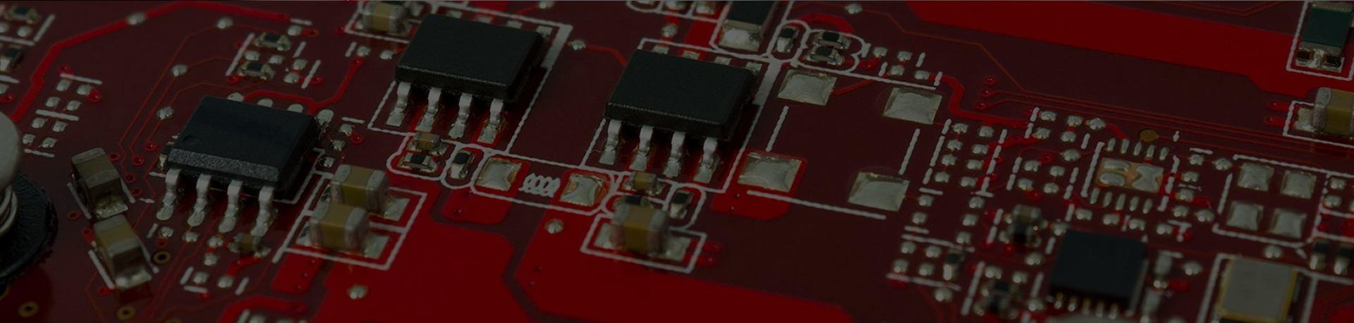
A Bluetooth PCB (Printed Circuit Board) consists of several components that work together to enable Bluetooth wireless communication. Here are the key components typically found on a Bluetooth circuit board:
• Bluetooth Module: The Bluetooth module is the core component responsible for Bluetooth communication. It includes the Bluetooth radio transceiver and associated circuitry. The module may be pre-built or integrated into the PCB as a surface-mounted device.
• Antenna: The antenna is essential for transmitting and receiving Bluetooth signals. It can be implemented as an embedded trace on the PCB or as a separate component, such as a chip antenna for an external antenna.
• Microcontroller or System-on-Chip (SoC): The microcontroller or SoC manages the overall operation of the Bluetooth circuit board. It handles tasks such as data processing, communication with the Bluetooth module, and interaction with other peripheral devices.
• Power Management Components: These components include voltage regulators, capacitors, and other power-related components to ensure stable and efficient power supply to the Bluetooth module and other circuitry on the PCB.
• Crystal Oscillator: A crystal oscillator provides the clock signal required for timing and synchronization of the Bluetooth module and associated circuitry.
• Supporting Passive and Active Components: Various passive components such as resistors, capacitors, inductors, and diodes are used for signal conditioning, filtering, and protection. Active components such as transistors and operational amplifiers may also be included depending on the specific requirements of the Bluetooth circuit board.
• Interfaces: The PCB may feature interface components such as UART (Universal Asynchronous Receiver-Transmitter), I2C (Inter-Integrated Circuit), SPI (Serial Peripheral Interface), or GPIO (General Purpose Input/Output) pins. These interfaces allow communication between the Bluetooth module and other devices or peripherals connected to the PCB.
• External Connectors: The Bluetooth PCB may include connectors, headers, or solder pads to establish external connections with other devices or peripherals. These connectors can facilitate power supply, data transfer, or control signals.
The specific components and their arrangement on a Bluetooth PCB board may vary depending on the design, functionality, and intended application of the Bluetooth device.
How to Design a Bluetooth PCB?
Designing a Bluetooth PCB (Printed Circuit Board) involves several steps and considerations to ensure proper functionality, signal integrity, and compatibility with Bluetooth standards. Here is a general overview of the process:
1. Define Requirements: Clearly define the requirements of your Bluetooth device. Consider factors such as the data rate, desired range, power consumption, form factor, and any specific features or interfaces needed.
2. Select Bluetooth Module: Choose a Bluetooth module that meets your requirements. Consider factors such as the Bluetooth version, supported profiles, output power, and antenna options. Ensure that the module is compatible with the necessary software development tools and documentation.
3. Determine PCB Specifications: Define the PCB specifications based on the Bluetooth module and other components. Consider factors such as layer count, size,
PCB material, and any special requirements for impedance control or high-speed signals.
4. Schematic Design: Create a schematic diagram that represents the connectivity and functionality of the Bluetooth circuit board. Place the Bluetooth module, power management components, microcontroller, interfaces, and other necessary components. Ensure proper connectivity and follow the manufacturer's guidelines for component placement and connections.
5. PCB Layout Design: Transfer the schematic design into the physical layout of the PCB. Carefully place the components, considering factors such as power distribution, signal integrity, and heat dissipation. Follow best practices for component placement, routing, and layer stack-up to minimize noise, impedance mismatch, and EMI issues. Consider the Bluetooth module's specific layout guidelines and keep RF traces as short and direct as possible.
6. Power and Ground Planes: Create solid power and ground planes to ensure proper power distribution and minimize noise. Separate analog and digital ground planes if required and connect them at a single point with low impedance.
7. Signal Integrity and EMI: Pay attention to signal integrity and EMI (Electromagnetic Interference) considerations. Properly route high-speed traces, use appropriate trace widths and spacing, and incorporate decoupling capacitors near power pins of ICs. Follow EMI shielding and grounding techniques as needed.
8. Antenna Design: If the Bluetooth PCB board requires an antenna, consider the type (embedded, chip, or external) and its placement. Ensure proper antenna matching and clearance from nearby components to optimize wireless performance.
9. Testing and Validation: Once the Bluetooth PCB is assembled, conduct thorough
functional testing and validation. Verify Bluetooth functionality, range, data transfer, and other performance parameters. Use appropriate test equipment and follow testing methodologies to ensure proper operation.
10. Regulatory Compliance: Ensure that your Bluetooth PCB board design complies with relevant regulatory standards and certifications, such as FCC (Federal Communications Commission) or CE (Conformité Européene). Perform tests, such as RF emissions testing, as required.
Sierra Assembly offers quality Bluetooth PCB assembly with excellent turnaround time and customer satisfaction.